

Introduction
Logic chips perform computations. These receive, carry out, and make decisions based on data. They are designed with complex architectures and billions of transistors for high performance. Some of the examples are CPUs, GPUs, ASICs, and SoCs. Data is stored in memory chips on a temporary (volatile) or permanent (non-volatile) basis. These are either volatile or nonvolatile. DRAM is for system memory, SRAM is for cache, and NOR flash is for code storage. For engineers, repetitive arrays of cells offer a high storage density.
Scope
- Explain the difference in the manufacturing processes.
- Describe the testing procedures of the logic chips and memory chips.
- Support the semiconductor device selection understanding.
Design Differences Between Logic Chips and Memory Chips
Logic chips perform operations including arithmetic calculations, decision-making, and signal processing. These are complex circuits comprising many interconnected components, frequently tuned for speed and flexibility. The main purpose of memory chips is data storage. Memory chips are built for the purpose of maximum storage density and reliability. Types of memory include volatile memory, like RAM, and non-volatile memory, like flash storage.
Visual Comparison of Chip Structures
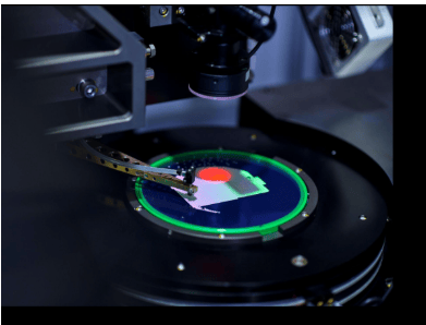
Manufacturing Differences
Logic chips use advanced fabrication processes with smaller transistor nodes to achieve high performance and speed. Such chips often require complex layouts in addition to numerous layers of interconnections. Memory chips, especially DRAM and NAND flash, provide high-density storage. Their production is based on the efficient stacking of cells and the minimization of cost per bit instead of providing the highest processing speed.
Testing Approaches
Logic Chip Testing
Engineers test the ability of the chip to execute the desired functions under varying circumstances. Techniques include:
- Engineers test chips to perform the necessary functions properly.
- Engineers determine signal delays for testing the chip speed.
- Fault detection and coverage
Memory Chip Testing
The focus of testing memory chips is to test data integrity and reliability. Engineers make sure that data can be written, stored, and retrieved in an accurate manner. Common methods include:
- Read/write cycle testing
- Retention testing
- Validation of error detection and correction.
Principle
The most important rule of both types of chips is based on semiconductor physics and electronic circuit design. Logic chips are built on transistor switching to process signals, while memory chips are built on charge-storage or state-retention mechanisms to store data.
Testing Procedure Overview
General testing steps for semiconductor devices include:
- Before packaging, wafer-level testing is done.
- Functional and parametric tests.
- Reliability testing (burn-in test).
- Final quality inspection.
These processes ensure that both logic and memory chips are able to achieve performance and reliability standards.
Significance
It is essential to know the differences between logic and memory chips in order to achieve maximum performance of the system. The adequate combination optimizes the speed, efficiency, and cost-effectiveness of electronic devices. It further helps manufacturers streamline production and quality control in the semiconductor lifecycle.
Applications
Logic and memory chips are used in a wide range of applications:
- Computers and laptops
- Smartphones and tablets
- Automotive electronics
- Industrial automation systems
- Data centers and cloud computing


