
Metals and Semiconductors

Metals and semiconductors are the backbone of modern industries and industrial development processes. These have immense usage is all walks of life including construction, medical devices, electronics, electrical gadgets and hundreds of other utilities. Semiconductor manufacturing utilizes rare earth metals such as Silicon and Germanium. Semiconductor research is the most focused are of research in the present world. Research and development activities involving metals and semiconductors need a variety of destructive and non-destructive testing.

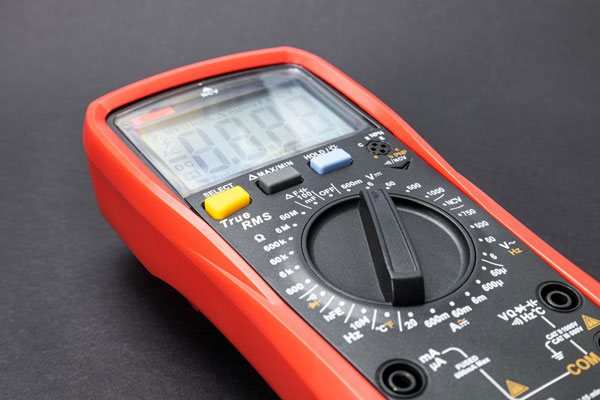
    Digital multimeter used for ASTM testing

    No results found.

    Metals and Metal Products Testing

    The malleability, ductility, strength, and temperature performance of metals makes them suitable for structural and load-bearing applications. Researchers are working to create metals, alloys, and composites that are strong, light, long-lasting, and corrosion-resistant. All ferrous and non-ferrous metals and alloys are tested for their mechanical properties, chemical composition, and metallographic properties. Other tests such as precision dimensional monitoring, nondestructive testing, fatigue testing, S-N curve, corrosion resistance testing, and environmental simulation tests are also done to ensure their quality and usability. Metal testing is done utilizing various methodologies to assess different parameters.

    Semiconductor Testing

    The semiconductor industry is a critical sector in the world economy that relies on rare earth metals for manufacturing electronic devices. Semiconductors are also known as integrated circuits, microelectronic chips, or computer chips. Semiconductors are tiny electronic devices based primarily on silicon or germanium. Semiconductors are composed of billions of components that can process, store, sense, and move data or signals. The main types of semiconductor chips are logic, memory, analog, optoelectronics, sensors, and discretes. Each of these types performs different functions and requires specialized design and manufacturing processes. Chip design, fabrication and manufacturing are the major activities taken up in the semiconductor industry. All research and manufacturing activities in this industry need various testing for quality assurance purposes.

    These are the major testing techniques utilized in semiconductor testing.
    1. Advanced microscopy
    2. Characterization of materials
    3. Surface analysis
    4. Trace elemental analysis
    5. Failure analysis
    6. Characterizing of dopants using SIMS
    7. Thin film analysis
    8. Particulate analysis
    9. Contamination analysis
    10. Visualizing surface morphology (AFM, XRR, Profilometry, Microscopy)

    FAQ

    Where can I get metals and semiconductors testing done?
    You can share your metals and semiconductors testing requirements with Matestlab. Matestlab has a vast network of material testing laboratories, spread across the USA and Canada. We support your all material testing needs ranging from specific metals and semiconductors tests to various testing techniques.
    Please contact us for a detailed quote for your metals and semiconductors testing needs. Cost incurred to carry out different metals and semiconductors testing methodology depends on the type of raw material; number of samples, coupons, or specimens; test conditions, turn around time etc. Please contact us for the best and latest prices.
    The required number of samples or specimens should comply with the relevant standard's procedure. The Matestlab operations team can assist you for your special requirements once you share your testing details with us.
    Matestlab has a vast testing laboratory network, hence we bring you the best testing facilities in a cost-effective way. We offer considerable discounts (15-20%) to our returning customers based on test volume and frequency.
    Turnaround time depends on the specific test procedure required. However, we at Matestlab understand your research requirements and hence try to get your testing completed within the least possible time.
    Testimonials
    Real results
    Engineers trust us with what matters most
    Why Choose Matestlab?
    Matestlab is a unified testing services partner based in the USA. Matestlab offers raw material and product testing services through accredited, expert laboratories primarily based in the USA. Matestlab supports physical, thermal, chemical, electrical, mechanical, environmental, and characterization testing needs through its global network of 2200+ accredited testing laboratories. Matestlab's in-house materials science experts curate and design comprehensive testing programs matched to the sample material and specific testing need, with regulatory requirements and confidentiality in mind.

    If you are looking for a managed and trusted testing partner to achieve your research goals, feel free to schedule a meeting with us or send us a request at connect@matestlabs.com to learn more about our services. For a quick quote, call us at (302)244-7710. We are happy to serve you.
    Start Your Testing
    Project Today
    Define your requirements and get access to
    specialized laboratories ready to deliver results
    Partners with us
    Clients
    Vendors
    Process for testing
    • STEP 01

      You share your testing requirements

    • STEP 02

      You share your sample(s)

    • STEP 03

      We deliver your test reports

    Get your testing done

    Let us know your testing requirements and we will be right back with a solution.

      Let us root for each other. Collaborate to grow, expand, and accelerate our businesses.

      Partner with us